






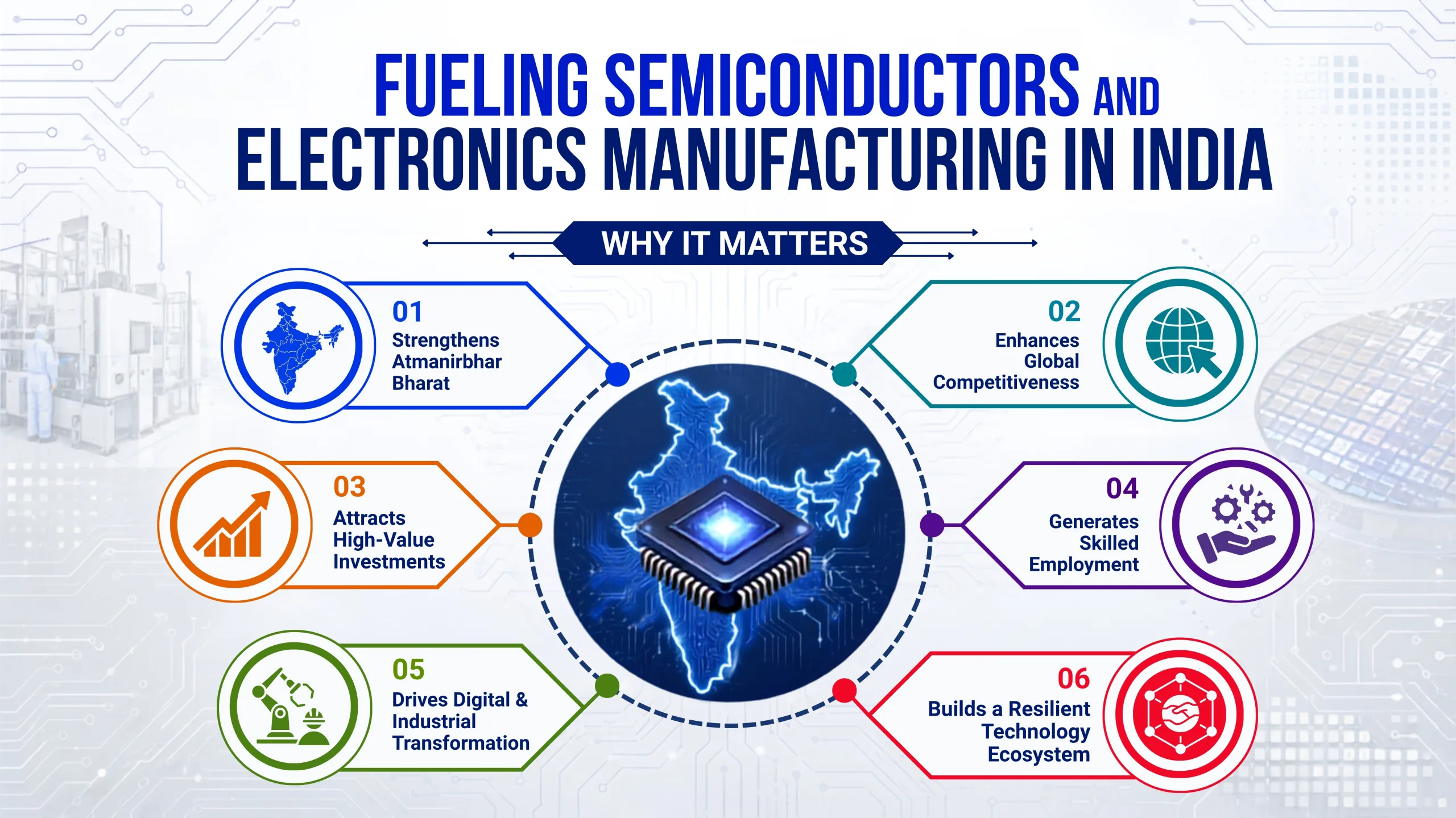
Geopolitical shifts, supply chain vulnerabilities, and the weaponization of critical minerals have forced international conglomerates to transition from efficiency-only supply chain models to resilience-led, multi-node frameworks. At the nexus of this transformation stands India. Driven by decisive policy interventions, robust domestic demand, and an aggressive push toward self-reliance (Aatmanirbhar Bharat), the landscape of electronics manufacturing in India has pivoted from basic low-value assembly to highly integrated, design-led ecosystem development.
As the PHD Chamber of Commerce and Industry (PHDCCI) observes, India is no longer just a consumer of technology- it is rapidly building the infrastructure to become a primary global producer. The cornerstone of this high-tech sovereign ambition is the evolution of a domestic semiconductor ecosystem in India. Driven by the landmark India Semiconductor Mission (ISM) and flanked by multi-billion-dollar fiscal frameworks like the Production Linked Incentive (PLI) scheme for electronics and the Electronics Components Manufacturing Scheme (ECMS), India is carving an indelible footprint on the global technology map.
This comprehensive strategic analysis breaks down the economic milestones, policy frameworks, operational blueprints, and structural challenges shaping India’s path toward a $500 billion domestic electronics ecosystem.
Evaluating India’s Electronics Manufacturing Boom
Over the past decade, India’s electronics manufacturing sector has scaled at an exponential trajectory. According to data released by the Press Information Bureau (PIB), domestic electronics production skyrocketed from ₹1.9 lakh crore in 2014-15 to an astonishing ₹11.3 lakh crore in 2024-25, representing a near six-fold expansion. Concurrently, sector-specific exports registered an eight-fold surge, jumping from ₹38,000 crore to ₹3.27 lakh crore within the same timeline. This industrial escalation has served as a primary economic engine, generating approximately 25 lakh jobs nationwide.
A significant portion of this success can be attributed to the spectacular turnaround in mobile communication hardware. In 2014, the nation operated a meager two mobile manufacturing units; today, it anchors over 300 highly advanced operational plants. While approximately 26% of mobile devices sold domestically were locally produced in 2014-15, that figure reached an unprecedented 99.2% by late 2024, signaling total import substitution and near complete self-reliance in mobile hardware. Mobile production alone surged 28-fold- from ₹18,000 crore in 2014-15 to ₹5.45 lakh crore in 2024-25- making India the second-largest mobile phone manufacturer across the globe.
According to latest industrial projections validated by KPMG and the Ministry of Electronics and Information Technology (MeitY), the Indian Electronic Manufacturing Services (EMS) market is on track to triple from its current baseline of $40-$45 billion to over $150 billion by FY30. This structural shift marks a vital maturation phase: transitioning from a high-volume assembly hub to an integrated manufacturing powerhouse with deep capabilities in value addition, component sourcing, and system-level intellectual property (IP).
Understanding the Policy Blueprint
India’s growth within the global electronics supply chain is not accidental; it is the direct byproduct of calculated, market-enabling policy architecture. The Government of India has deployed a multi-tiered fiscal incentive matrix designed to neutralize disabilities, achieve massive economies of scale, and de-risk early-stage capital expenditure for global and domestic investors.
Production Linked Incentive (PLI) Framework
The master framework remains the Production-Linked Incentive (PLI) Scheme, backed by an aggregate budget outlay of ₹1.9 lakh crore across 14 strategic sectors. The PLI Scheme for Large-Scale Electronics Manufacturing offers an incentive of 3% to 6% on incremental sales of goods manufactured within domestic boundaries. As of early 2025, this specific scheme alone has attracted a cumulative investment exceeding ₹10,905 crore, translating into a massive cumulative production volume of ₹7,15,823 crore and driving direct employment for nearly 1.4 lakh citizens.
Electronics Components Manufacturing Scheme (ECMS)
While high-level system assembly drives headline numbers, a sustainable Electronics System Design and Manufacturing (ESDM) environment is impossible without localized component manufacturing. Addressing this structural gap, the government notified the Electronics Components Manufacturing Scheme (ECMS) on April 8, 2025. Originally established with a baseline outlay of ₹22,919 crore, the scheme targets deep-tier manufacturing- including capacitors, resistors, printed circuit boards (PCBs), and active sub-assemblies.
Recognizing the overwhelming investor appetite, where investment commitments quickly reached ₹1,15,351 crore (nearly double the initial target), the Union Budget 2026-27 dramatically expanded the policy framework by accelerating the overall financial allocation to ₹40,000 crore. ECMS provides deep turnover-linked, capex, and hybrid fiscal cushions to ensure domestic component ecosystems integrate seamlessly into global value chains, with expectations to generate over ₹10.34 lakh crore in production value over the next six years.
Decoding India Semiconductor Mission (ISM) 1.0 and 2.0
Semiconductors represent the structural nervous system of modern industrial economies, undergirding everything from high-performance computing, artificial intelligence, and telecommunications networks to automotive electronics and defense systems. To mitigate vulnerability to localized geopolitical chokepoints, the Union Cabinet rolled out the India Semiconductor Mission (ISM) 1.0 with a foundational corpus of ₹76,000 crore, offering standard 50% fiscal support on a pari-passu basis for silicon fabrication units, compound semiconductor plants, display fabs, and OSAT/ATMP infrastructures.
Building aggressively on this momentum, the Union Budget 2026-27 introduced the highly anticipated India Semiconductor Mission 2.0 (ISM 2.0). While ISM 1.0 focused on establishing foundational fabrication and packaging facilities, ISM 2.0 addresses the upstream and downstream supply dependencies.
Key Focus Areas of ISM 2.0:
- Equipment & Materials Localization: Developing local capacity for high-purity chemicals, gases, photoresists, and specialized manufacturing equipment.
- Full-Stack Indian IP Ownership: Supporting the creation of domestic semiconductor Intellectual Property (IP) and advanced EDA (Electronic Design Automation) tools.
- Supply Chain Fortification: Securing reliable logistics, resilient power matrices, and ultra-pure water channels to ensure uninterrupted fab operations.
- Industry-Led R&D and Workforce Training: Allocating a targeted ₹1,000 crore push for FY2026-27 toward building dedicated research institutes and advanced engineering centers.
The ultimate roadmap under the evolving Semicon framework is clear: advancing beyond mature nodes to achieve commercial production capability in 3-nanometer (nm) and 2-nanometer cutting-edge technology nodes, securing India’s place among the elite tier of global semiconductor nations by 2035.
The Commercial Landmarks of 2026
- Micron Technology (Sanand, Gujarat): In February 2026, Micron officially commenced commercial production at its landmark Semiconductor Assembly, Test, and Packaging (ATMP) facility in Sanand, Gujarat. This facility represents the frontline of India’s high-density memory packaging capability.
- Kaynes Semicon (Sanand, Gujarat): Closely following Micron, Kaynes Semicon operationalized its state-of-the-art OSAT (Outsourced Semiconductor Assembly and Test) plant in March 2026, boosting daily output for automotive, industrial, and consumer applications.
- Tata Electronics Fab (Dholera, Gujarat): Progressing rapidly via a strategic technology partnership with Taiwan’s Powerchip Semiconductor Manufacturing Corporation (PSMC), this ₹91,526 crore mega project is transforming the Dholera semiconductor hub into India’s premier silicon valley, focusing on mature nodes (28nm to 90nm) that cater to power management, display drivers, and automotive controllers.
- CG Power & Renesas OSAT (Sanand, Gujarat): A joint venture with Renesas Electronics America and Stars Microelectronics, this facility boasts a projected capacity of 15.07 million units per day.
- Advanced 3D Packaging Infrastructure (Bhubaneswar, Odisha): April 2026 marked the formal groundbreaking of India’s first Advanced Heterogeneous Integration Packaging Solutions (3DGS) unit in Odisha, providing a direct hardware catalyst for AI, 5G, and advanced defense systems.
- New Additions (May 2026 Approvals): The Cabinet greenlit Crystal Matrix, an integrated compound semiconductor fab and ATMP unit in Dholera, and Suchi Semicon, a specialized OSAT infrastructure in Surat, expanding Gujarat’s manufacturing footprint.
The Design Ecosystem: From DLI Scheme to Global IP Creation
India has long been the unsung backbone of global chip design; nearly 20% of the world’s semiconductor design engineers operate out of engineering hubs in Bengaluru, Hyderabad, Noida, and Pune. However, this talent historically generated IP for foreign multinationals. Through the Design Linked Incentive (DLI) Scheme, the India Semiconductor Mission is shifting this balance by nurturing homegrown startups.
As of mid-2026, the DLI scheme supports 24 active semiconductor design startups, which have successfully raised nearly ₹430 crore in venture capital funding. The academic-industrial linkage has yielded phenomenal dividends: over 67,000 students and 1,000 startup engineers are utilizing advanced EDA chip design software tools provided via national infrastructure.
In academic labs, 122 chip designs have been taped out, with 56 chips successfully fabricated at 180nm at the Semiconductor Laboratory (SML) in Mohali. More impressively, chip startups have completed 16 successful tape-outs, resulting in six specialized microchips fabricated at advanced international foundry nodes down to 12nm, signaling India’s rapid climb up the technological value chain.
Strategic Challenges: The Roadblocks India Must Navigate
Despite the immense macro-economic tailwinds, the path to total tech sovereignty demands rigorous problem-solving. Semiconductor and Electronics manufacturing is arguably the most capital-intensive, complex, and resource-sensitive industry on earth. PHDCCI identifies four critical structural challenges that require synchronized intervention:
- High Input Import Dependency: Across high-end electronics and chip packaging, import dependency for core materials ranges between 80% to 95%. Localizing the sub-component supply chain via ECMS is crucial to prevent value-addition leakage.
- Ultra-Pure Resource Logistics: A standard silicon fab requires millions of gallons of ultra-pure water daily, a perfectly uninterrupted, baseline power matrix (where even a microsecond voltage fluctuation can ruin an entire wafer lot), and vibration-isolated logistics corridors.
- The Advanced Skill Gap: While India possesses a vast base of digital and software engineering talent, fabricating chips requires highly specialized metallurgical, chemical, and physical hardware engineering expertise.
- Global Incentive Competition: The US CHIPS Act, the European Chips Act, and massive subsidy frameworks across East Asia create a highly competitive environment for securing global foreign direct investment (FDI).
Our Recommendations
To secure India’s position as a reliable, trusted, and highly competitive node in the global electronics value chain, PHDCCI advocates for a forward-looking, multi-pronged industry approach:
- Accelerating State-Level Policy Alignment: State governments must complement central incentives with fast-tracked land allocations, guaranteed zero-fluctuation power grids, and dedicated water recycling systems tailored for ESDM clusters.
- Deepening Academic-Industry Integration: Launching micro-specializations and dual-degree vocational certifications in semiconductor manufacturing processes across premier technical institutes (IITs, NITs) to secure a steady workforce pipeline.
- Structuring a Common Equipment & Materials Sandbox: Establishing localized special economic zones (SEZs) focused strictly on raw inputs (silicon wafers, specialty gases, precision cleanroom apparel) to drastically compress logistical lead times for operational fabs.
- Boosting Domestic Procurement Channels: Encouraging domestic public and private enterprises to absorb homegrown chip designs and components, ensuring a reliable local market for early-stage domestic innovators.
India’s electronic and semiconductor trajectory has definitively crossed the inflection point. By moving decisively up the complexity curve from basic device assembly to deep-tech silicon fabrication, the nation is actively insulating its economy against supply chain disruptions while establishing a foundational pillar for global technological leadership. Through concerted execution, policy stability, and deep public-private collaboration, the silicon renaissance is officially underway.